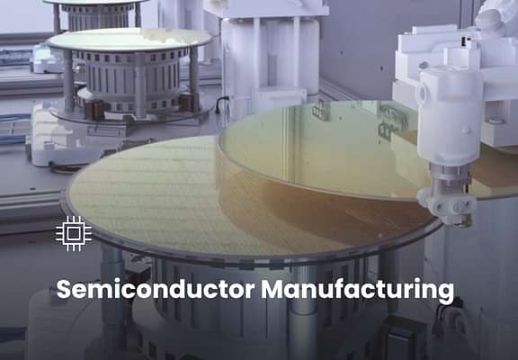
Advancing Semiconductor Manufacturing and PCBs

In the highly specialized fields of semiconductor manufacturing and printed circuit board (PCB) production, the demand for precision and efficiency is at an all-time high. As technology advances, and components shrink to the nanometer scale, margins for error narrow. In this context, Vision AI is emerging as a transformative technology, reshaping how manufacturers approach quality control and operational efficiency.
Vision AI, at its core, leverages deep learning algorithms to analyze visual data from production lines in real time. Unlike traditional inspection methods, which rely heavily on human oversight or rudimentary automation, Vision AI systems are capable of detecting microscopic defects and anomalies with remarkable accuracy. This is particularly crucial in semiconductor manufacturing, where even the slightest imperfection can compromise the performance of an entire chip or circuit.
Key contributions of Vision AI to semiconductor and PCB manufacturing include:
Automated Real-Time Inspection: Vision AI systems continuously monitor production environments, capturing and analyzing high-resolution images to identify defects. These systems outperform human inspectors by detecting flaws that may be invisible to the naked eye, such as minute misalignments or surface imperfections at the microscopic level.
Enhanced Precision and Accuracy: Semiconductor wafers and PCBs consist of intricate and densely packed microstructures. Vision AI allows for the precise inspection of solder joints, component placements, and conductive traces. Its ability to detect sub-micron level discrepancies makes it indispensable in ensuring that each component meets exact specifications.
Yield Optimization: A critical advantage of Vision AI is its capacity to detect defects early in the manufacturing process. By identifying problems at the earliest possible stage, manufacturers can minimize waste, reduce rework, and optimize overall yield. This directly impacts both the efficiency of production lines and the bottom line of manufacturers.
Scalability and Adaptability: Vision AI systems are highly adaptable and can be scaled across multiple production lines. Moreover, they are flexible enough to accommodate evolving manufacturing processes, ensuring that they remain effective even as the complexity of semiconductor designs increases.
As semiconductor manufacturing moves toward ever greater levels of complexity, Vision AI is poised to play a central role in advancing the field. The combination of deep learning and advanced image processing allows manufacturers to maintain the rigorous quality standards necessary for today’s cutting-edge technology. From optimizing throughput to reducing production costs, Vision AI is not just a tool for quality control — it is a catalyst for manufacturing innovation.
The future of semiconductor and PCB production will depend on these intelligent systems, as they enable unprecedented levels of precision and operational efficiency. It explains why Vision AI represents a significant leap forward, aligning manufacturing capabilities with the rapid pace of technological progress.